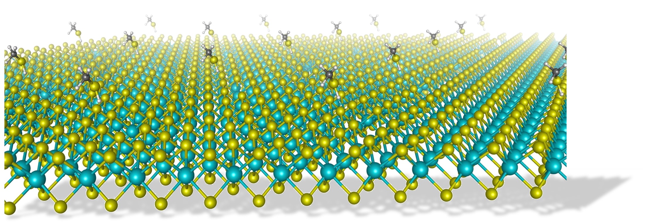
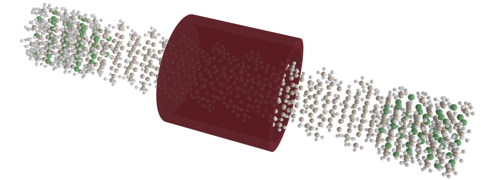
Simulation and modeling of nano membranes, hybrid materials and interfaces
operated by the MAIN simulation groups of Prof. Sibylle Gemming sibylle.gemming@… and Dr. Jörg Schuster joerg.schuster@…
Charge transport in membranes and at interfaces
- Simulation of charge transfer in 2D hetero structures
- Network models of graphene based conductor materials
- Hopping transport models for organic polymers
Functionalization and processing of membranes and low dimensional materials
- Models of chemically functionalized 2D-materials
- Simulation of thin film processing (CVD, ALD, PVD, etch ...)
Electronic structure of nano materials
- Simulation of electronic carbon nano devices
- Transistor models for interface controlled devices
- Random alloy models for Si/Ge and related materials
- Properties of real nano materials: role of strain and defects
Principal investigators
Prof. Dr. Sibylle GemmingInstitute of physics Quantum Mechanical Processes and Systems sibylle.gemming@…
|
Dr. Jörg SchusterCenter for Microtechnologies Simulation of processes, materials and devices joerg.schuster@…
|
 |
 |


