31. Diagramme (-40 … +85 °C)
Die nachfolgenden Diagramme zeigen das typische Verhalten.
Diese Daten sind nicht getestet.
Alle Stromverbrauchs-Messungen wurden durchgeführt
als alle I/O-Pins als Eingang konfiguriert
und die internen pull-up-Widerstände freigegeben waren.
Als Taktquelle wurde ein Rechteckgenerator mit Rail-to-Rail-Ausgang verwendet.
Alle Verbräuche wurden gemessen, wenn alle Bits im PRR-Register gesetzt wurden
und damit alle Peripherieeinheiten deaktiviert wurden.
Außerdem wurde der Analogvergleicher abgeschaltet.
Siehe ATmega88: Stromverbrauch der I/O-Module
um den zusätzlichen Stromverbrauch der jeweiligen I/O-Module
hinzuzurechnen.
Der Stromverbrauch im Leistung-weg-Modus ist unabhängig von der Taktquelle.
Der Stromverbrauch hängt von verschiedenen Faktoren ab:
Der Versorgungsspannung, der Taktfrequenz, den Zuständen an den I/O-Pins,
der Schaltrate der I/O-Pins, dem ausgeführten Befehl
und der Umgebungstemperatur.
Die wesentlichen Faktoren sind die Versorgungsspannung und die Taktfrequenz.
Der Stromverbrauch eines kapazitiv belasteten Pins kann abgeschätzt werden
mit CL · UCC · f,
wobei CL der Kapazität, UCC der Versorgungsspannung
und f der Schaltfrequenz des I/O-Pins entspricht.
Die Diagramme enthalten Frequenzen, die höher sind als die Testlimits.
Die Chips garantieren aber keine korrekte Funktion bei Frequenzen
oberhalb des in der Bestellbezeichnung angegebenen Wertes.
Die Differenz beim Stromverbrauch zwischen Leistung-weg-Modus
mit und ohne freigegebenen Watchdog entspricht dem Stromverbrauch des Watchdogs.
31.1 Diagramme ATmega48A
31.1.1 Strom unter Last
Bild 31-1: ATmega48A: Strom unter Last vs. Frequenz (0,1 – 1,0 MHz)
Bild 31-2: ATmega48A: Strom unter Last vs. Frequenz (1 - 20 MHz

Bild 31-3: ATmega48A: Strom unter Last vs. UCC (Interner RC-Oszillator, 128kHz)

Bild 31-4: ATmega48A: Strom unter Last vs. UCC (Interner RC-Oszillator, 1 MHz)

Bild 31-5: ATmega48A: Strom unter Last vs. UCC (Interner RC-Oszillator, 8 MHz)

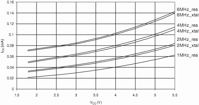
31.1.2 Stromaufnahme im Leerlauf
Bild 31-6: ATmega48A: Stromaufnahme im Leerlauf vs. Frequenz (0,1 – 1,0 MHz)

Bild 31-7: ATmega48A: Stromaufnahme im Leerlauf vs. Frequenz (1 – 20 MHz)

Bild 31-8: ATmega48A: Stromaufnahme im Leerlauf vs. UCC (Interner RC-Oszillator, 128kHz)

Bild 31-9: ATmega48A: Stromaufnahme im Leerlauf vs. UCC (Interner RC-Oszillator, 1 MHz)

Bild 31-10: ATmega48A: Stromaufnahme im Leerlauf vs. UCC (Interner RC-Oszillator, 8 MHz)

31.1.3 ATmega48A: Stromaufnahme der I/O-Module
Die folgenden Tabellen und Formeln können zur Berechnung der zusätzlichen Stromaufnahme der verschiedenen I/O-Module unter Last und im Leerlauf herangezogen werden.
Das Freigeben und Sperren der I/O-Module wird über das Leistungs-Reduktions-Register gesteuert.
It is possible to calculate the typical current consumption based on the numbers from Tabelle 31-2
for other UCC und frequency settings than listed in Tabelle 31-1.
31.1.3.1 Beispiel
Berechne die zu erwartende Stromaufnahme im Leerlauf mit TIMER1, ADU und SPI bei UCC = 2,0 V und F = 1 MHz:
Von Tabelle 31-4, dritte Spalte, we see that we need to add 11,2 % for the TIMER1,
22.1 % for the ADU und 17,6 % for the SPI module. Reading from Bild 31-53, we find that the idle
current consumption is ≈0,028 mA at UCC = 2,0 V und F = 1 MHz. Die Gesamtstromaufnahme im Leerlauf mit
TIMER1, ADU und SPI enabled, gives:
ICCtotal ≈ 0,028 mA ∙(1 + 0,112 + 0,221 + 0.176) ≈ 0,042 mA
Tabelle 31-1: ATmega48PA: Zusätzlicher Stromverbrauch der verschiedenen I/O-Module, in µA
| PRR-Bit | Typische Werte
|
|---|
| UCC = 2 V, F = 1 MHz | UCC = 3 V, F = 4 MHz | UCC = 5 V, F = 8 MHz
|
|---|
| PRUSART0 | 2,9 µA | 20,7 µA | 97,4 µA
|
| PRTWI | 6,0 µA | 44,8 µA | 219,7 µA
|
| PRTIM2 | 5,0 µA | 34,5 µA | 141,3 µAµA
|
| PRTIM1 | 3,6 µA | 24,4 µA | 107,7 µA
|
| PRTIM0 | 1,4 µA | 9,5 µA | 38,4 µA
|
| PRSPI | 5,0 µA | 38,0 µA | 190,4 µA
|
| PRADC | 6,1 µA | 47,4 µA | 244,7 µA
|
Tabelle 31-2: ATmega48PA: Zusätzlicher Stromverbrauch (in Prozent) unter Last und im Leerlauf
| PRR-Bit
| Zusätzlicher Stromverbrauch verglichen mit CPU-Last und externem Takt (siehe Bild 31-48 und Bild 31-49)
| Zusätzlicher Stromverbrauch verglichen mit Leerlauf und externem Takt (siehe Bild 31-53 und Bild 31-54)
|
|---|
| PRUSART0 | 1,8 % | 11,4 %
|
| PRTWI | 3,9 % | 20,6 %
|
| PRTIM2 | 2,9 % | 15,7 %
|
| PRTIM1 | 2,1 % | 11,2 %
|
| PRTIM0 | 0,8 % | 4,2 %
|
| PRSPI | 3,3 % | 17,6 %
|
| PRADC | 4,2 % | 22,1 %
|
31.1.4 Stromaufnahme bei Leistung-weg
Bild 31-11: ATmega48A: Stromaufnahme bei Leistung-weg vs. UCC (Watchdog deaktiviert)

Bild 31-12: ATmega48A: Stromaufnahme bei Leistung-weg vs. UCC (Watchdog aktiviert)

31.1.5 Stromaufnahme beim Leistung sparen
Bild 31-13: ATmega48A: Stromaufnahme beim Leistung sparen vs. UCC (Watchdog deaktiviert und 32kHz Crystal Oscillator Running)

31.1.6 Stromaufnahme in Bereitschaft
Bild 31-14: ATmega48A: Stromaufnahme in Bereitschaft vs. UCC (Watchdog deaktiviert)

31.1.7 Pin-Pullups
Bild 31-15: ATmega48A: Strom durch Pullup-Widerstand vs. Eingangsspannung (UCC = 1,8 V)

Bild 31-16: ATmega48A: Strom durch Pullup-Widerstand vs. Eingangsspannung (UCC = 2,7 V)

Bild 31-17: ATmega48A: Strom durch Pullup-Widerstand vs. Eingangsspannung (UCC = 5 V)
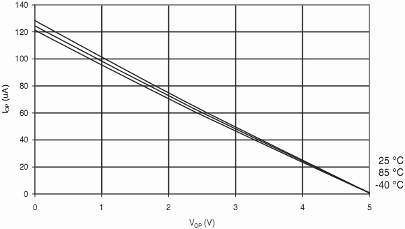
Bild 31-18: ATmega48A: Strom durch Pullup-Widerstand vs. Spannung am RESET-Pin (UCC = 1,8 V))

Bild 31-19: ATmega48A: Strom durch Pullup-Widerstand vs. Spannung am RESET-Pin (V = 2,7 V)

Bild 31 – 20: ATmega48A: Strom durch Pullup-Widerstand vs. Spannung am RESET-Pin (UCC = 5 V)

31.1.8 Treiberstärke der Pins
Bild 31-21: ATmega48A: Ausgangsspannung vs. Strom nach Masse am I/O-Pin (UCC = 3 V)

Bild 31-22: ATmega48A: Ausgangsspannung vs. Strom nach Masse am I/O-Pin (UCC = 5 V)

Bild 31-23: ATmega48A: Ausgangsspannung vs. Strom von UCC am I/O-Pin (UCC = 3 V)

Bild 31-24: ATmega48A: Ausgangsspannung vs. Strom von UCC am I/O-Pin (UCC = 5 V)

31.1.9 Schaltschwelle und Hysterese der Pins
Bild 31-25: ATmega48A: Schaltschwelle vs. UCC (UIH, Pin liest „1“)

Bild 31-26: ATmega48A: Schaltschwelle vs. UCC (UIL, Pin liest „0“)

Bild 31-27: ATmega48A: Hysterese vs. UCC

Bild 31-28: ATmega48A: Schaltschwelle vs. UCC am RESET-Pin (UIH, Pin liest „1“)

Bild 31-29: ATmega48A: Schaltschwelle vs. UCC am RESET-Pin (UIL, Pin liest „0“)

Bild 31-30: ATmega48A: Hysterese vs. UCC am RESET-Pin

31.1.10 Unterspannungsdetektor-Schwelle
Bild 31-31: ATmega48A: Schaltschwellen des Unterspannungsdetektors vs. Temperatur (BODLEVEL = 1,8 V)

Bild 31-32: ATmega48A: Schaltschwellen des Unterspannungsdetektors vs. Temperatur (BODLEVEL = 2,7 V)

Bild 31-33: ATmega48A: Schaltschwellen des Unterspannungsdetektors vs. Temperatur (BODLEVEL = 4,3 V)

Bild 31-34: ATmega48A: Referenzspannung vs. UCC

31.1.11 Interner Oszillator
Bild 31-35: ATmega48A: Watchdog-Oszillatorfrequenz vs. Temperatur

Bild 31-36: ATmega48A: Watchdog-Oszillatorfrequenz vs. UCC

Bild 31-37: ATmega48A: Kalibrierte 8-MHz-RC-Oszillatorfrequenz vs. UCC

Bild 31-38: ATmega48A: Kalibrierte 8-MHz-RC-Oszillatorfrequenz vs. Temperatur

Bild 31-39: ATmega48A: Kalibrierte 8-MHz-RC-Oszillatorfrequenz vs. OSCCAL-Wert

31.1.12 Verbrauch der I/O-Module
Bild 31-40: ATmega48A: Stromaufnahme des A/D-Wandlers vs. UCC (AREF = AUCC)

Bild 31-41: ATmega48A: Stromaufnahme des Analogvergleichers vs. UCC

Bild 31-42: ATmega48A: Strom der externen Spannungsreferenz AREF vs. UCC

Bild 31-43: ATmega48A Stromaufnahme des Unterspannungsdetektor vs. UCC

Bild 31-44: ATmega48A: Programmierstrom vs. UCC

31.1.13 Reset-Verbrauch und -Pulsbreite
Bild 31-45: ATmega48A: Stromaufnahme während Reset vs. Frequenz (0.1 - 1,0 MHz)

Bild 31-46: ATmega48A: Stromaufnahme während Reset vs. Frequenz (1 - 20 MHz)

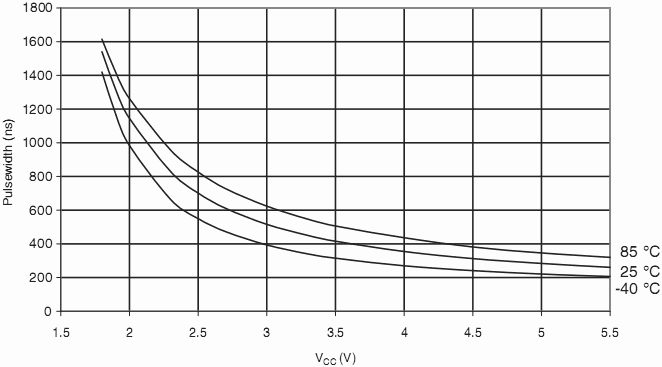
Bild 31-47: ATmega48A: Minimale Resetpulsbreite vs. UCC

31.2 Diagramme ATmega48PA
31.2.1 Strom unter Last
Bild 31-48: ATmega48PA: Strom unter Last vs. Frequenz (0,1 – 1,0 MHz)

Bild 31-49: ATmega48PA: Strom unter Last vs. Frequenz (1 – 20 MHz)

Bild 31-50: ATmega48PA: Strom unter Last vs. UCC (Interner RC-Oszillator, 128kHz)

Bild 31-51: ATmega48PA: Strom unter Last vs. UCC (Interner RC-Oszillator, 1 MHz)

Bild 31-52: ATmega48PA: Strom unter Last vs. UCC (Interner RC-Oszillator, 8 MHz)

31.2.2 Stromaufnahme im Leerlauf
Bild 31-53: ATmega48PA: Stromaufnahme im Leerlauf vs. Frequenz (0,1 – 1,0 MHz)

Bild 31-54: ATmega48PA: Stromaufnahme im Leerlauf vs. Frequenz (1 – 20 MHz)

Bild 31-55: ATmega48PA: Stromaufnahme im Leerlauf vs. UCC (Interner RC-Oszillator, 128kHz)

Bild 31-56: ATmega48PA: Stromaufnahme im Leerlauf vs. UCC (Interner RC-Oszillator, 1 MHz)

Bild 31-57: ATmega48PA: Stromaufnahme im Leerlauf vs. UCC (Interner RC-Oszillator, 8 MHz)

31.2.3 ATmega48PA: Stromaufnahme der I/O-Module
Die folgenden Tabellen und Formeln können zur Berechnung der zusätzlichen Stromaufnahme der verschiedenen I/O-Module unter Last und im Leerlauf herangezogen werden.
Das Freigeben und Sperren der I/O-Module wird über das Leistungs-Reduktions-Register gesteuert.
It is possible to calculate the typical current consumption based on the numbers from Tabelle 31-4
for other UCC und frequency settings than listed in Tabelle 31-3.
Tabelle 31-3: ATmega48PA: Zusätzlicher Stromverbrauch der verschiedenen I/O-Module, in µA
| PRR-Bit | Typische Werte
|
|---|
| UCC = 2 V, F = 1 MHz | UCC = 3 V, F = 4 MHz | UCC = 5 V, F = 8 MHz
|
|---|
| PRUSART0 | 2,9 µA | 20,7 µA | 97,4 µA
|
| PRTWI | 6,0 µA | 44,8 µA | 219,7 µA
|
| PRTIM2 | 5,0 µA | 34,5 µA | 141,3 µA
|
| PRTIM1 | 3,6 µA | 24,4 µA | 107,7 µA
|
| PRTIM0 | 1,4 µA | 9,5 µA | 38,4 µA
|
| PRSPI | 5,0 µA | 38,0 µA | 190,4 µA
|
| PRADC | 6,1 µA | 47,4 µA | 244,7 µA
|
Tabelle 31-4: ATmega48PA: Zusätzlicher Stromverbrauch (in Prozent) unter Last und im Leerlauf
| PRR-Bit
| Zusätzlicher Stromverbrauch verglichen mit CPU-Last und externem Takt (siehe Bild 31-48 und Bild 31-49)
| Zusätzlicher Stromverbrauch verglichen mit Leerlauf und externem Takt (siehe Bild 31-53 und Bild 31-54)
|
|---|
| PRUSART0 | 1,8 % | 11,4 %
|
| PRTWI | 3,9 % | 20,6 %
|
| PRTIM2 | 2,9 % | 15,7 %
|
| PRTIM1 | 2,1 % | 11,2 %
|
| PRTIM0 | 0,8 % | 4,2 %
|
| PRSPI | 3,3 % | 17,6 %
|
| PRADC | 4,2 % | 22,1 %
|
31.2.3.1 Beispiel
Berechne die zu erwartende Stromaufnahme im Leerlauf mit TIMER1, ADU und SPI bei UCC = 2,0 V und F = 1 MHz:
Von Tabelle 31-4, dritte Spalte, we see that we need to add 11,2 % for the TIMER1,
22.1 % for the ADU und 17,6 % for the SPI module. Reading from Bild 31-53, we find that the idle
current consumption is ≈0,028 mA at UCC = 2,0 V und F = 1 MHz. Die Gesamtstromaufnahme im Leerlauf mit
TIMER1, ADU und SPI enabled, gives:
ICCtotal ≈ 0,028 mA ∙(1 + 0,112 + 0,221 + 0.176) ≈ 0,042 mA
31.2.4 Stromaufnahme bei Leistung-weg
Bild 31-58: ATmega48PA: Stromaufnahme bei Leistung-weg vs. UCC (Watchdog deaktiviert)

Bild 31-59: ATmega48PA: Stromaufnahme bei Leistung-weg vs. UCC (Watchdog aktiviert)

31.2.5 Stromaufnahme beim Leistung sparen
Bild 31-60: ATmega48PA: Stromaufnahme beim Leistung sparen vs. UCC (Watchdog deaktiviert und 32kHz Crystal Oscillator Running)

31.2.6 Stromaufnahme in Bereitschaft
Bild 31-61: ATmega48PA: Stromaufnahme in Bereitschaft vs. UCC (Watchdog deaktiviert)

31.2.7 Pin-Pullups
Bild 31-62: ATmega48PA: Strom durch Pullup-Widerstand vs. Eingangsspannung (UCC = 1,8 V)

Bild 31-63: ATmega48PA: Strom durch Pullup-Widerstand vs. Eingangsspannung (UCC = 2,7 V)

Bild 31-64: ATmega48PA: Strom durch Pullup-Widerstand vs. Eingangsspannung (UCC = 5 V)

Bild 31-65: ATmega48PA: Strom durch Pullup-Widerstand vs. Spannung am RESET-Pin (UCC = 1,8 V)

Bild 31-66: ATmega48PA: Strom durch Pullup-Widerstand vs. Spannung am RESET-Pin (UCC = 2,7 V)

Bild 31-67: ATmega48PA: Strom durch Pullup-Widerstand vs. Spannung am RESET-Pin (UCC = 5 V)

31.2.8 Treiberstärke der Pins
Bild 31-68: ATmega48PA: Ausgangsspannung vs. Strom nach Masse am I/O-Pin (UCC = 3 V)

Bild 31-69: ATmega48PA: Ausgangsspannung vs. Strom nach Masse am I/O-Pin (V = 5 V)

Bild 31-70: ATmega48PA: Ausgangsspannung vs. Strom von UCC am I/O-Pin (UCC = 3 V)

Bild 31-71: ATmega48PA: Ausgangsspannung vs. Strom von UCC am I/O-Pin (UCC = 5 V)

31.2.9 Schaltschwelle und Hysterese der Pins
Bild 31-72: ATmega48PA: Schaltschwelle vs. UCC (UIH, Pin liest „1“)

Bild 31-73: ATmega48PA: Schaltschwelle vs. UCC (UIL, Pin liest „0“)

Bild 31-74: ATmega48PA: Hysterese vs. UCC

Bild 31-75: ATmega48PA: Schaltschwelle vs. UCC am RESET-Pin (UIH, Pin liest „1“)

Bild 31-76: ATmega48PA: Schaltschwelle vs. UCC am RESET-Pin (UIL, Pin liest „0“)

Bild 31-77: ATmega48PA: Hysterese vs. UCC am RESET-Pin

31.2.10 Unterspannungsdetektor-Schwelle
Bild 31-78: ATmega48PA: Schaltschwellen des Unterspannungsdetektors vs. Temperatur (BODLEVEL = 1,8 V)

Bild 31-79: ATmega48PA: Schaltschwellen des Unterspannungsdetektors vs. Temperatur (BODLEVEL = 2,7 V)

Bild 31-80: ATmega48PA: Schaltschwellen des Unterspannungsdetektors vs. Temperatur (BODLEVEL = 4,3 V)

Bild 31-81: ATmega48PA: Referenzspannung vs. UCC

31.2.11 Interner Oszillator
Bild 31-82: ATmega48PA: Watchdog-Oszillatorfrequenz vs. Temperatur
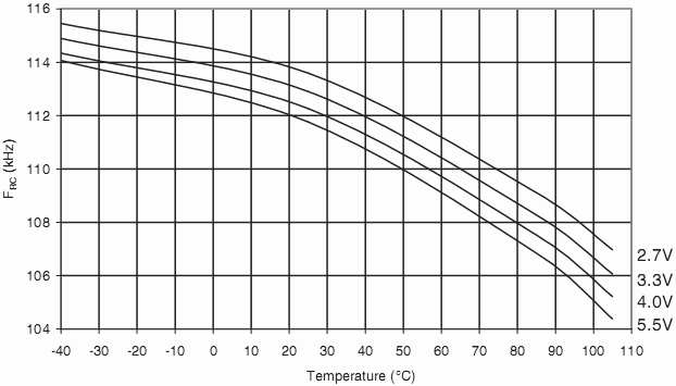
Bild 31-83: ATmega48PA: Watchdog-Oszillatorfrequenz vs. UCC

Bild 31-84: ATmega48PA: Kalibrierte 8-MHz-RC-Oszillatorfrequenz vs. UCC

Bild 31-85: ATmega48PA: Kalibrierte 8-MHz-RC-Oszillatorfrequenz vs. Temperatur

Bild 31-86: ATmega48PA: Kalibrierte 8-MHz-RC-Oszillatorfrequenz vs. OSCCAL-Wert

31.2.12 Verbrauch der I/O-Module
Bild 31-87: ATmega48PA: Stromaufnahme des A/D-Wandlers vs. UCC (AREF = AUCC)

Bild 31-88: ATmega48PA: Stromaufnahme des Analogvergleichers vs. UCC

Bild 31-89: ATmega48PA: Strom der externen Spannungsreferenz AREF vs. UCC

Bild 31-90: ATmega48PA: Stromaufnahme des Unterspannungsdetektor vs. UCC

Bild 31-91: ATmega48PA: Programmierstrom vs. UCC

31.2.13 Reset-Verbrauch und -Pulsbreite
Bild 31-92: ATmega48PA: Stromaufnahme während Reset vs. Frequenz (0.1 MHz- 1,0 MHz)

Bild 31-93: ATmega48PA: Stromaufnahme während Reset vs. Frequenz (1 MHz- 20 MHz)

Bild 31-94: ATmega48PA: Minimale Resetpulsbreite vs. UCC

31.3 Diagramme ATmega88A
31.3.1 Strom unter Last
Bild 31-95: ATmega88A: Strom unter Last vs. Frequenz (0,1 – 1,0 MHz)

Bild 31-96: ATmega88A: Strom unter Last vs. Frequenz (1 - 20 MHz)

Bild 31-97: ATmega88A: Strom unter Last vs. UCC (Interner RC-Oszillator, 128kHz)

Bild 31-98: ATmega88A: Strom unter Last vs. UCC (Interner RC-Oszillator, 1 MHz)

Bild 31-99: ATmega88A: Strom unter Last vs. UCC (Interner RC-Oszillator, 8 MHz)

31.3.2 Stromaufnahme im Leerlauf
Bild 31-100: ATmega88A: Stromaufnahme im Leerlauf vs. Frequenz (0,1 – 1,0 MHz)

Bild 31-101: ATmega88A: Stromaufnahme im Leerlauf vs. Frequenz (1 – 20 MHz)

Bild 31-102: ATmega88A: Stromaufnahme im Leerlauf vs. UCC (Interner RC-Oszillator, 128kHz)

Bild 31-103: ATmega88A: Stromaufnahme im Leerlauf vs. UCC (Interner RC-Oszillator, 1 MHz)
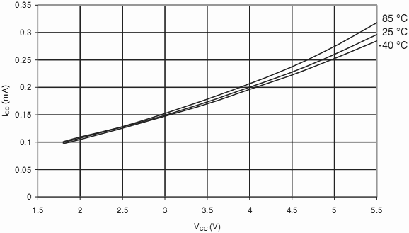
Bild 31-104: ATmega88A: Stromaufnahme im Leerlauf vs. UCC (Interner RC-Oszillator, 8 MHz)

31.3.3 ATmega88A: Stromaufnahme der I/O-Module
Die folgenden Tabellen und Formeln können zur Berechnung der zusätzlichen Stromaufnahme der verschiedenen I/O-Module unter Last und im Leerlauf herangezogen werden.
Das Freigeben und Sperren der I/O-Module wird über das Leistungs-Reduktions-Register gesteuert.
Tabelle 31-5: ATmega88A: Zusätzlicher Stromverbrauch der verschiedenen I/O-Module, in µA
| PRR-Bit | Typische Werte
|
|---|
| UCC = 2 V, F = 1 MHz | UCC = 3 V, F = 4 MHz | UCC = 5 V, F = 8 MHz
|
|---|
| PRUSART0 | 3,0 µA | 21,3 µA | 97,9 µA
|
| PRTWI | 6,1 µA | 45,4 µA | 219,0 µA
|
| PRTIM2 | 5,2 µA | 35,2 µA | 149,5 µA
|
| PRTIM1 | 3,8 µA | 25,6 µA | 110,0 µA
|
| PRTIM0 | 1,5 µA | 9,8 µA | 39,6 µA
|
| PRSPI | 5,2 µA | 40,0 µA | 199,6 µA
|
| PRADC | 6,3 µA | 48,7 µA | 247,0 µA
|
Tabelle 31-6: ATmega88A: Zusätzlicher Stromverbrauch (in Prozent) unter Last und im Leerlauf
| PRR-Bit
| Zusätzlicher Stromverbrauch verglichen mit CPU-Last und externem Takt (siehe Bild 31-142 und Bild 31-143)
| Zusätzlicher Stromverbrauch verglichen mit Leerlauf und externem Takt (siehe Bild 31-147 und Bild 31-148)
|
|---|
| PRUSART0 | 1,8 % | 11,4 %
|
| PRTWI | 3,9 % | 24,4 %
|
| PRTIM2 | 2,9 % | 18,6 %
|
| PRTIM1 | 2,1 % | 13,6 %
|
| PRTIM0 | 0,8 % | 5,2 %
|
| PRSPI | 3,5 % | 21,5 %
|
| PRADC | 4,2 % | 26,3 %
|
It is possible to calculate the typical current consumption based on the numbers from Tabelle 31-8
for other UCC und frequency settings than listed in Tabelle 31-7.
31.3.3.1 Beispiel
Berechne die zu erwartende Stromaufnahme im Leerlauf mit TIMER1, ADU und SPI bei UCC = 2,0 V und F = 1 MHz:
Von Tabelle 31-8, dritte Spalte, we see that we need to add 13,6 % for the TIMER1,
26.3 % for the ADU und 21,5 % for the SPI module. Reading from Bild 31-147, we find that the
idle current consumption is ≈0,027 mA at UCC = 2,0 V und F = 1 MHz. The total current consumption in idle mode
with TIMER1, ADU und SPI enabled, gives:
ICCtotal ≈ 0,027 mA ∙(1 + 0,136 + 0,263 + 0.215) ≈ 0,043 mA
31.3.4 Stromaufnahme bei Leistung-weg
Bild 31-105: ATmega88A: Stromaufnahme bei Leistung-weg vs. UCC (Watchdog deaktiviert)
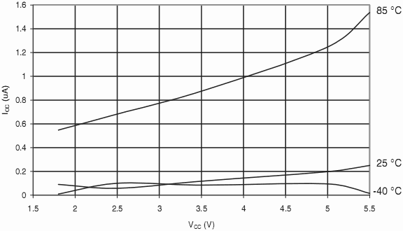
Bild 31-106: ATmega88A: Stromaufnahme bei Leistung-weg vs. UCC (Watchdog aktiviert)

31.3.5 Stromaufnahme beim Leistung sparen
Bild 31-107: ATmega88A: Stromaufnahme beim Leistung sparen vs. UCC (Watchdog deaktiviert und 32kHz Crystal Oscillator Running)

31.3.6 Stromaufnahme in Bereitschaft
Bild 31-108: ATmega88A: Stromaufnahme in Bereitschaft vs. UCC (Watchdog deaktiviert)

31.3.7 Pin-Pullups
Bild 31-109: ATmega88A: Strom durch Pullup-Widerstand vs. Eingangsspannung (UCC = 1,8 V)

Bild 31-110: ATmega88A: Strom durch Pullup-Widerstand vs. Eingangsspannung (UCC = 2,7 V)

Bild 31-111: ATmega88A: Strom durch Pullup-Widerstand vs. Eingangsspannung (UCC = 5 V)

Bild 31-112: ATmega88A: Strom durch Pullup-Widerstand vs. Spannung am RESET-Pin (UCC = 1,8 V)

Bild 31-113: ATmega88A: Strom durch Pullup-Widerstand vs. Spannung am RESET-Pin (UCC = 2,7 V)

Bild 31-114: ATmega88A: Strom durch Pullup-Widerstand vs. Spannung am RESET-Pin (UCC = 5 V)

31.3.8 Treiberstärke der Pins
Bild 31-115: ATmega88A: Ausgangsspannung vs. Strom nach Masse am I/O-Pin (UCC = 3 V)

Bild 31-116: ATmega88A: Ausgangsspannung vs. Strom nach Masse am I/O-Pin (UCC = 5 V)

Bild 31-117: ATmega88A: Ausgangsspannung vs. Strom von UCC am I/O-Pin (UCC = 3 V)

Bild 31-118: ATmega88A: Ausgangsspannung vs. Strom von UCC am I/O-Pin (UCC = 5 V)

31.3.9 Schaltschwelle und Hysterese der Pins
Bild 31-119: ATmega88A: Schaltschwelle vs. UCC (UIH, Pin liest „1“)

Bild 31-120: ATmega88A: Schaltschwelle vs. UCC (UIL, Pin liest „0“)

Bild 31-121: ATmega88A: Hysterese vs. UCC

Bild 31-122: ATmega88A: Schaltschwelle vs. UCC am RESET-Pin (UIH, Pin liest „1“)

Bild 31-123: ATmega88A: Schaltschwelle vs. UCC am RESET-Pin (UIL, Pin liest „0“)

Bild 31-124: ATmega88A: Hysterese vs. UCC am RESET-Pin

31.3.10 Unterspannungsdetektor-Schwelle
Bild 31-125: ATmega88A: Schaltschwellen des Unterspannungsdetektors vs. Temperatur (BODLEVEL = 1,8 V)

Bild 31-126: ATmega88A: Schaltschwellen des Unterspannungsdetektors vs. Temperatur (BODLEVEL = 2,7 V)

Bild 31-127: ATmega88A: Schaltschwellen des Unterspannungsdetektors vs. Temperatur (BODLEVEL = 4,3 V)

Bild 31-128: ATmega88A: Referenzspannung vs. UCC

31.3.11 Interner Oszillator
Bild 31-129: ATmega88A: Watchdog-Oszillatorfrequenz vs. Temperatur

Bild 31-130: ATmega88A: Watchdog-Oszillatorfrequenz vs. UCC

Bild 31-131: ATmega88A: Kalibrierte 8-MHz-RC-Oszillatorfrequenz vs. UCC

Bild 31-132: ATmega88A: Kalibrierte 8-MHz-RC-Oszillatorfrequenz vs. Temperatur

Bild 31-133: ATmega88A: Kalibrierte 8-MHz-RC-Oszillatorfrequenz vs. OSCCAL-Wert

31.3.12 Verbrauch der I/O-Module
Bild 31-134: ATmega88A: Stromaufnahme des A/D-Wandlers vs. UCC (AREF = AUCC)

Bild 31-135: ATmega88A: Stromaufnahme des Analogvergleichers vs. UCC

Bild 31-136: ATmega88A: Strom der externen Spannungsreferenz AREF vs. UCC

Bild 31-137: ATmega88A: Stromaufnahme des Unterspannungsdetektor vs. UCC

Bild 31-138: ATmega88A: Programmierstrom vs. UCC

31.3.13 Reset-Verbrauch und -Pulsbreite
Bild 31-139: ATmega88A: Stromaufnahme während Reset vs. Frequenz (0.1 - 1,0 MHz)

Bild 31-140: ATmega88A: Stromaufnahme während Reset vs. Frequenz (1 - 20 MHz)

Bild 31-141: ATmega88A: Minimale Resetpulsbreite vs. UCC

31.4 Diagramme ATmega88PA
31.4.1 Strom unter Last
Bild 31-142: ATmega88PA: Strom unter Last vs. Frequenz (0,1 – 1,0 MHz)
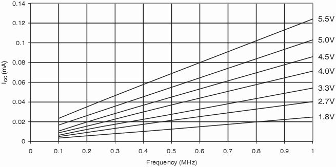
Bild 31-143: ATmega88PA: Strom unter Last vs. Frequenz (1 - 20 MHz)

Bild 31-144: ATmega88PA: Strom unter Last vs. UCC (Interner RC-Oszillator, 128kHz)

Bild 31-145: ATmega88PA: Strom unter Last vs. UCC (Interner RC-Oszillator, 1 MHz)

Bild 31-146: ATmega88PA: Strom unter Last vs. UCC (Interner RC-Oszillator, 8 MHz)

31.4.2 Stromaufnahme im Leerlauf
Bild 31-147: ATmega88PA: Stromaufnahme im Leerlauf vs. Frequenz (0,1 – 1,0 MHz)

Bild 31-148: ATmega88PA: Stromaufnahme im Leerlauf vs. Frequenz (1 - 20 MHz)

Bild 31-149: ATmega88PA: Stromaufnahme im Leerlauf vs. UCC (Interner RC-Oszillator, 128kHz)

Bild 31-150: ATmega88PA: Stromaufnahme im Leerlauf vs. UCC (Interner RC-Oszillator, 1 MHz)

Bild 31-151: ATmega88PA: Stromaufnahme im Leerlauf vs. UCC (Interner RC-Oszillator, 8 MHz)

31.4.3 ATmega88PA: Stromaufnahme der I/O-Module
Die folgenden Tabellen und Formeln können zur Berechnung der zusätzlichen Stromaufnahme der verschiedenen I/O-Module unter Last und im Leerlauf herangezogen werden.
Das Freigeben und Sperren der I/O-Module wird über das Leistungs-Reduktions-Register gesteuert.
Tabelle 31-7: ATmega88PA: Zusätzlicher Stromverbrauch der verschiedenen I/O-Module, in µA
| PRR-Bit | Typische Werte
|
|---|
| UCC = 2 V, F = 1 MHz | UCC = 3 V, F = 4 MHz | UCC = 5 V, F = 8 MHz
|
|---|
| PRUSART0 | 3,0 µA | 21,3 µA | 97,9 µA
|
| PRTWI | 6,1 µA | 45,4 µA | 219,0 µA
|
| PRTIM2 | 5,2 µA | 35,2 µA | 149,5 µA
|
| PRTIM1 | 3,8 µA | 25,6 µA | 110,0 µA
|
| PRTIM0 | 1,5 µA | 9,8 µA | 39,6 µA
|
| PRSPI | 5,2 µA | 40,0 µA | 199,6 µA
|
| PRADC | 6,3 µA | 48,7 µA | 247,0 µA
|
Tabelle 31-8: ATmega88PA: Zusätzlicher Stromverbrauch (in Prozent) unter Last und im Leerlauf
| PRR-Bit
| Zusätzlicher Stromverbrauch verglichen mit CPU-Last und externem Takt (siehe Bild 31-142 und Bild 31-143)
| Zusätzlicher Stromverbrauch verglichen mit Leerlauf und externem Takt (siehe Bild 31-147 und Bild 31-148)
|
|---|
| PRUSART0 | 1,8 % | 11,4 %
|
| PRTWI | 3,9 % | 24,4 %
|
| PRTIM2 | 2,9 % | 18,6 %
|
| PRTIM1 | 2,1 % | 13,6 %
|
| PRTIM0 | 0,8 % | 5,2 %
|
| PRSPI | 3,5 % | 21,5 %
|
| PRADC | 4,2 % | 26,3 %
|
It is possible to calculate the typical current consumption based on the numbers from Tabelle 31-8 for other UCC und frequency settings than listed in Tabelle 31-7.
31.4.3.1 Beispiel
Berechne die zu erwartende Stromaufnahme im Leerlauf mit TIMER1, ADU und SPI bei UCC = 2,0 V und F = 1 MHz:
Von Tabelle 31-8, dritte Spalte, we see that we need to add 13,6 % for the TIMER1, 26,3 % for the
ADU und 21,5 % for the SPI module. Reading from Bild 31-147, we find that the idle current
consumption is ≈0,027 mA at UCC = 2,0 V und F = 1 MHz. Die Gesamtstromaufnahme im Leerlauf mit
TIMER1, ADU und SPI enabled, gives:
ICCtotal ≈ 0,027 mA ∙(1 + 0,136 + 0,263 + 0.215) ≈ 0,043 mA
31.4.4 Stromaufnahme bei Leistung-weg
Bild 31-152: ATmega88PA: Stromaufnahme bei Leistung-weg vs. UCC (Watchdog deaktiviert)

Bild 31-153: ATmega88PA: Stromaufnahme bei Leistung-weg vs. UCC (Watchdog aktiviert)

31.4.5 Stromaufnahme beim Leistung sparen
Bild 31-154: ATmega88PA: Stromaufnahme beim Leistung sparen vs. UCC (Watchdog deaktiviert und 32kHz Crystal Oscillator Running)

31.4.6 Stromaufnahme in Bereitschaft
Bild 31-155: ATmega88PA: Stromaufnahme in Bereitschaft vs. UCC (Watchdog deaktiviert)

31.4.7 Pin-Pullups
Bild 31-156: ATmega88PA: Strom durch Pullup-Widerstand vs. Eingangsspannung (UCC = 1,8 V)

Bild 31-157: ATmega88PA: Strom durch Pullup-Widerstand vs. Eingangsspannung (UCC = 2,7 V)

Bild 31-158: ATmega88PA: Strom durch Pullup-Widerstand vs. Eingangsspannung (UCC = 5 V)

Bild 31-159: ATmega88PA: Strom durch Pullup-Widerstand vs. Spannung am RESET-Pin (UCC = 1,8 V)

Bild 31-160: ATmega88PA: Strom durch Pullup-Widerstand vs. Spannung am RESET-Pin (UCC = 2,7 V)

Bild 31-161: ATmega88PA: Strom durch Pullup-Widerstand vs. Spannung am RESET-Pin (UCC = 5 V)

31.4.8 Treiberstärke der Pins
Bild 31-162: ATmega88PA: Ausgangsspannung vs. Strom nach Masse am I/O-Pin (UCC = 3 V)

Bild 31-163: ATmega88PA: Ausgangsspannung vs. Strom nach Masse am I/O-Pin (UCC = 5 V)

Bild 31-164: ATmega88PA: Ausgangsspannung vs. Strom von UCC am I/O-Pin (UCC = 3 V)

Bild 31-165: ATmega88PA: Ausgangsspannung vs. Strom von UCC am I/O-Pin (UCC = 5 V)

31.4.9 Schaltschwelle und Hysterese der Pins
Bild 31-166: ATmega88PA: Schaltschwelle vs. UCC (UIH, Pin liest „1“)

Bild 31-167: ATmega88PA: Schaltschwelle vs. UCC (UIL, Pin liest „0“)

Bild 31-168: ATmega88PA: Hysterese vs. UCC

Bild 31-169: ATmega88PA: Schaltschwelle vs. UCC am RESET-Pin (UIH, Pin liest „1“)

Bild 31-170: ATmega88PA: Schaltschwelle vs. UCC am RESET-Pin (UIL, Pin liest „0“)

Bild 31-171: ATmega88PA: Hysterese vs. UCC am RESET-Pin

31.4.10 Unterspannungsdetektor-Schwelle
Bild 31-172: ATmega88PA: Schaltschwellen des Unterspannungsdetektors vs. Temperatur (BODLEVEL = 1,8 V)

Bild 31-173: ATmega88PA: Schaltschwellen des Unterspannungsdetektors vs. Temperatur (BODLEVEL = 2,7 V)

Bild 31-174: ATmega88PA: Schaltschwellen des Unterspannungsdetektors vs. Temperatur (BODLEVEL = 4,3 V)

Bild 31-175: ATmega88PA: Kalibrierte Referenzspannung vs. Temperatur

Bild 31-176: ATmega88PA: Referenzspannung vs. UCC

31.4.11 Interner Oszillator
Bild 31-177: ATmega88PA: Watchdog-Oszillatorfrequenz vs. Temperatur

Bild 31-178: ATmega88PA: Watchdog-Oszillatorfrequenz vs. UCC

Bild 31-179: ATmega88PA: Kalibrierte 8-MHz-RC-Oszillatorfrequenz vs. UCC

Bild 31-180: ATmega88PA: Kalibrierte 8-MHz-RC-Oszillatorfrequenz vs. Temperatur

Bild 31-181: ATmega88PA: Kalibrierte 8-MHz-RC-Oszillatorfrequenz vs. OSCCAL-Wert

31.4.12 Verbrauch der I/O-Module
Bild 31-182: ATmega88PA: Stromaufnahme des A/D-Wandlers vs. UCC (AREF = AUCC)

Bild 31-183: ATmega88PA: Stromaufnahme des Analogvergleichers vs. UCC

Bild 31-184: ATmega88PA: Strom der externen Spannungsreferenz AREF vs. UCC

Bild 31-185: ATmega88PA: Stromaufnahme des Unterspannungsdetektor vs. UCC

Bild 31-186: ATmega88PA: Programmierstrom vs. UCC

31.4.13 Reset-Verbrauch und -Pulsbreite
Bild 31-187: ATmega88PA: Stromaufnahme während Reset vs. Frequenz (0,1 – 1,0 MHz)

Bild 31-188: ATmega88PA: Stromaufnahme während Reset vs. Frequenz (1 - 20 MHz)

Bild 31-189: ATmega88PA: Minimale Resetpulsbreite vs. UCC

31.5 Diagramme ATmega168A
31.5.1 Strom unter Last
Bild 31-190: ATmega168A: Strom unter Last vs. Frequenz (0,1 – 1,0 MHz)

Bild 31-191: ATmega168A: Strom unter Last vs. Frequenz (1 – 20 MHz)

Bild 31-192: ATmega168A: Strom unter Last vs. UCC (Interner RC-Oszillator, 128kHz)

Bild 31-193: ATmega168A: Strom unter Last vs. UCC (Interner RC-Oszillator, 1 MHz)
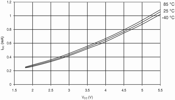
Bild 31-194: ATmega168A: Strom unter Last vs. UCC (Interner RC-Oszillator, 8 MHz)

31.5.2 Stromaufnahme im Leerlauf
Bild 31-195: ATmega168A: Stromaufnahme im Leerlauf vs. Frequenz (0,1 – 1,0 MHz)

Bild 31-196: ATmega168A: Stromaufnahme im Leerlauf vs. Frequenz (1 – 20 MHz)

Bild 31-197: IATmega168A: Stromaufnahme im Leerlauf vs. UCC (Interner RC-Oszillator, 128kHz)

Bild 31-198: ATmega168A: Stromaufnahme im Leerlauf vs. UCC (Interner RC-Oszillator, 1 MHz)

Bild 31-199: ATmega168A: Stromaufnahme im Leerlauf vs. UCC (Interner RC-Oszillator, 8 MHz)

31.5.3 ATmega168A Stromaufnahme der I/O-Module
Die folgenden Tabellen und Formeln können zur Berechnung der zusätzlichen Stromaufnahme der verschiedenen I/O-Module unter Last und im Leerlauf herangezogen werden.
Das Freigeben und Sperren der I/O-Module wird über das Leistungs-Reduktions-Register gesteuert.
Tabelle 31-9: ATmega168A: Zusätzlicher Stromverbrauch der verschiedenen I/O-Module, in µA
| PRR-Bit | Typische Werte
|
|---|
| UCC = 2 V, F = 1 MHz | UCC = 3 V, F = 4 MHz | UCC = 5 V, F = 8 MHz
|
|---|
| PRUSART0 | 2,86 µA | 20,3 µA | 52,2 µA
|
| PRTWI | 6,00 µA | 44,1 µA | 122,0 µA
|
| PRTIM2 | 4,97 µA | 33,2 µA | 79,8 µA
|
| PRTIM1 | 3,50 µA | 23,0 µA | 55,3 µA
|
| PRTIM0 | 1,43 µA | 9,2 µA | 21,4 µA
|
| PRSPI | 5,01 µA | 38,6 µA | 111,4 µA
|
| PRADC | 6,34 µA | 45,7 µA | 123,6 µA
|
Tabelle 31-10: ATmega168A: Zusätzlicher Stromverbrauch (in Prozent) unter Last und im Leerlauf
| PRR-Bit
| Zusätzlicher Stromverbrauch verglichen mit CPU-Last und externem Takt (siehe Bild 31-237 und Bild 31-238)
| Zusätzlicher Stromverbrauch verglichen mit Leerlauf und externem Takt (siehe Bild 31-242 und Bild 31-243)
|
|---|
| PRUSART0 | 1,5 % | 8,9 %
|
| PRTWI | 3,2 % | 19,5 %
|
| PRTIM2 | 2,4 % | 14,8 %
|
| PRTIM1 | 1,7 % | 10,3 %
|
| PRTIM0 | 0,7 % | 4,1 %
|
| PRSPI | 2,9 % | 17,1 %
|
| PRADC | 3,4 % | 20,3 %
|
It is possible to calculate the typical current consumption based on the numbers from Tabelle 31-12
for other UCC und frequency settings than listed in Tabelle 31-11.
31.5.3.1 Beispiel
Berechne die zu erwartende Stromaufnahme im Leerlauf mit TIMER1, ADU und SPI bei UCC = 2,0 V und F = 1 MHz:
Von Tabelle 31-12, dritte Spalte, we see that we need to add 10,3 % for the
TIMER1, 20,3 % for the ADU und 17,1 % for the SPI module. Reading from Bild 31-242, we find
that the idle current consumption is ≈0,027 mA at UCC = 2,0 V und F = 1 MHz. The total current consumption in
idle mode with TIMER1, ADU und SPI enabled, gives:
ICCtotal ≈ 0,027 mA ∙(1 + 0,103 + 0,203 + 0,171) ≈ 0,040 mA
31.5.4 Stromaufnahme bei Leistung-weg
Bild 31 – 200: ATmega168A: Stromaufnahme bei Leistung-weg vs. UCC (Watchdog deaktiviert)

Bild 31 – 201: ATmega168A: Stromaufnahme bei Leistung-weg vs. UCC (Watchdog aktiviert)

31.5.5 Stromaufnahme beim Leistung sparen
Bild 31 – 202: ATmega168A: Stromaufnahme beim Leistung sparen vs. UCC (Watchdog deaktiviert und 32kHz Crystal Oscillator Running)

31.5.6 Stromaufnahme in Bereitschaft
Bild 31 – 203: ATmega168A: Stromaufnahme in Bereitschaft vs. UCC (Watchdog deaktiviert)

31.5.7 Pin-Pullups
Bild 31 – 204: ATmega168A: Strom durch Pullup-Widerstand vs. Eingangsspannung (UCC = 1,8 V)

Bild 31 – 205: ATmega168A: Strom durch Pullup-Widerstand vs. Eingangsspannung (UCC = 2,7 V)
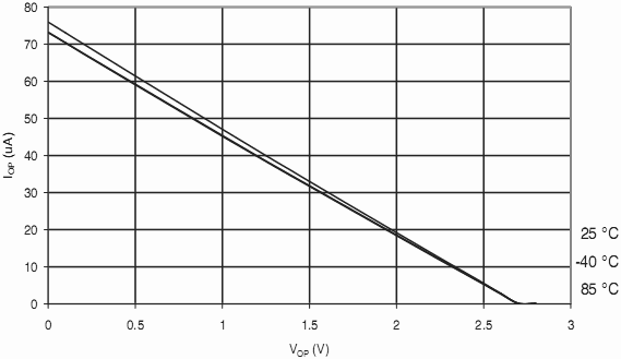
Bild 31 – 206: ATmega168A: Strom durch Pullup-Widerstand vs. Eingangsspannung (UCC = 5 V)

Bild 31 – 207: ATmega168A: Strom durch Pullup-Widerstand vs. Spannung am RESET-Pin (UCC =1.8 V)
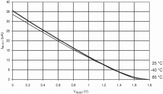
Bild 31 – 208: ATmega168A: Strom durch Pullup-Widerstand vs. Spannung am RESET-Pin (UCC =2.7 V)

Bild 31 – 209: ATmega168A: Strom durch Pullup-Widerstand vs. Spannung am RESET-Pin (UCC =5 V)

31.5.8 Treiberstärke der Pins
Bild 31-210: ATmega168A: Ausgangsspannung vs. Strom nach Masse am I/O-Pin (UCC = 3 V)

Bild 31-211: ATmega168A: Ausgangsspannung vs. Strom nach Masse am I/O-Pin (UCC = 5 V)

Bild 31-212: ATmega168A: Ausgangsspannung vs. Strom von UCC am I/O-Pin (UCC = 3 V)

Bild 31-213: ATmega168A: Ausgangsspannung vs. Strom von UCC am I/O-Pin (UCC = 5 V)

31.5.9 Schaltschwelle und Hysterese der Pins
Bild 31-214: ATmega168A: Schaltschwelle vs. UCC (UIH, Pin liest „1“)

Bild 31-215: ATmega168A: Schaltschwelle vs. UCC (UIL, Pin liest „0“)

Bild 31-216: ATmega168A: Hysterese vs. UCC

Bild 31-217: ATmega168A: Schaltschwelle vs. UCC am RESET-Pin (UIH, Pin liest „1“)

Bild 31-218: ATmega168A: Schaltschwelle vs. UCC am RESET-Pin (UIL, Pin liest „0“)

Bild 31-219: ATmega168A: Hysterese vs. UCC am RESET-Pin

31.5.10 Unterspannungsdetektor-Schwelle
Bild 31-220: ATmega168A: Schaltschwellen des Unterspannungsdetektors vs. Temperatur (BODLEVEL = 1,8 V)

Bild 31-221: ATmega168A: Schaltschwellen des Unterspannungsdetektors vs. Temperatur (BODLEVEL = 2,7 V)

Bild 31-222: ATmega168A: Schaltschwellen des Unterspannungsdetektors vs. Temperatur (BODLEVEL = 4,3 V)

Bild 31-223: ATmega168A: Referenzspannung vs. UCC

31.5.11 Interner Oszillator
Bild 31-224: ATmega168A: Watchdog-Oszillatorfrequenz vs. Temperatur

Bild 31-225: ATmega168A: Watchdog-Oszillatorfrequenz vs. UCC

Bild 31-226: ATmega168A: Kalibrierte 8-MHz-RC-Oszillatorfrequenz vs. UCC

Bild 31-227: ATmega168A: Kalibrierte 8-MHz-RC-Oszillatorfrequenz vs. Temperatur

Bild 31-228: ATmega168A: Kalibrierte 8-MHz-RC-Oszillatorfrequenz vs. OSCCAL-Wert

31.5.12 Verbrauch der I/O-Module
Bild 31-229: ATmega168A: Stromaufnahme des A/D-Wandlers vs. UCC (AREF = AUCC)

Bild 31-230: ATmega168A: Stromaufnahme des Analogvergleichers vs. UCC

Bild 31-231: ATmega168A: Strom der externen Spannungsreferenz AREF vs. UCC

Bild 31-232: ATmega168A: Stromaufnahme des Unterspannungsdetektor vs. UCC

Bild 31-233: ATmega168A: Programmierstrom vs. UCC

31.5.13 Reset-Verbrauch und -Pulsbreite
Bild 31-234: ATmega168A: Stromaufnahme während Reset vs. Frequenz (0.1 - 1,0 MHz)

Bild 31-235: ATmega168A: Stromaufnahme während Reset vs. Frequenz (1 - 20 MHz)

Bild 31-236: ATmega168A: Minimale Resetpulsbreite vs. UCC

31.6 Diagramme ATmega168PA
31.6.1 Strom unter Last
Bild 31-237: ATmega168PA: Strom unter Last vs. Frequenz (0,1 – 1,0 MHz)

Bild 31-238: ATmega168PA: Strom unter Last vs. Frequenz (1 – 20 MHz)

Bild 31-239: ATmega168PA: Strom unter Last vs. UCC (Interner RC-Oszillator, 128kHz)
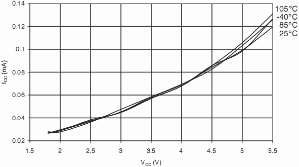
Bild 31-240: ATmega168PA: Strom unter Last vs. UCC (Interner RC-Oszillator, 1 MHz)

Bild 31-241: ATmega168PA: Strom unter Last vs. UCC (Interner RC-Oszillator, 8 MHz)

31.6.2 Stromaufnahme im Leerlauf
Bild 31-242: ATmega168PA: Stromaufnahme im Leerlauf vs. Frequenz (0,1 – 1,0 MHz)

Bild 31-243: ATmega168PA: Stromaufnahme im Leerlauf vs. Frequenz (1 – 20 MHz)

Bild 31-244: ATmega168PA: Stromaufnahme im Leerlauf vs. UCC (Interner RC-Oszillator, 128kHz)
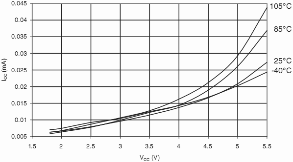
Bild 31-245: ATmega168PA: Stromaufnahme im Leerlauf vs. UCC (Interner RC-Oszillator, 1 MHz)

Bild 31-246: ATmega168PA: Stromaufnahme im Leerlauf vs. UCC (Interner RC-Oszillator, 8 MHz)

31.6.3 ATmega168PA Stromaufnahme der I/O-Module
Die folgenden Tabellen und Formeln können zur Berechnung der zusätzlichen Stromaufnahme der verschiedenen I/O-Module unter Last und im Leerlauf herangezogen werden.
Das Freigeben und Sperren der I/O-Module wird über das Leistungs-Reduktions-Register gesteuert.
Tabelle 31-11: ATmega168PA: Zusätzlicher Stromverbrauch der verschiedenen I/O-Module, in µA
| PRR-Bit | Typische Werte
|
|---|
| UCC = 2 V, F = 1 MHz | UCC = 3 V, F = 4 MHz | UCC = 5 V, F = 8 MHz
|
|---|
| PRUSART0 | 2,86 µA | 20,3 µA | 52,2 µA
|
| PRTWI | 6,00 µA | 44,1 µA | 122,0 µA
|
| PRTIM2 | 4,97 µA | 33,2 µA | 79,8 µA
|
| PRTIM1 | 3,50 µA | 23,0 µA | 55,3 µA
|
| PRTIM0 | 1,43 µA | 9,2 µA | 21,4 µA
|
| PRSPI | 5,01 µA | 38,6 µA | 111,4 µA
|
| PRADC | 6,34 µA | 45,7 µA | 123,6 µA
|
Tabelle 31-12: ATmega168PA: Zusätzlicher Stromverbrauch (in Prozent) unter Last und im Leerlauf
| PRR-Bit
| Zusätzlicher Stromverbrauch verglichen mit CPU-Last und externem Takt (siehe Bild 31-237 und Bild 31-238)
| Zusätzlicher Stromverbrauch verglichen mit Leerlauf und externem Takt (siehe Bild 31-242 und Bild 31-243)
|
|---|
| PRUSART0 | 1,5 % | 8,9 %
|
| PRTWI | 3,2 % | 19,5 %
|
| PRTIM2 | 2,4 % | 14,8 %
|
| PRTIM1 | 1,7 % | 10,3 %
|
| PRTIM0 | 0,7 % | 4,1 %
|
| PRSPI | 2,9 % | 17,1 %
|
| PRADC | 3,4 % | 20,3 %
|
It is possible to calculate the typical current consumption based on the numbers from Tabelle 31-12
for other UCC und frequency settings than listed in Tabelle 31-11.
31.6.3.1 Beispiel
Berechne die zu erwartende Stromaufnahme im Leerlauf mit TIMER1, ADU und SPI bei UCC = 2,0 V und F = 1 MHz:
Von Tabelle 31-12, dritte Spalte, we see that we need to add 10,3 % for the
TIMER1, 20,3 % for the ADU und 17,1 % for the SPI module. Reading from Bild 31-242, we find
that the idle current consumption is ≈0,027 mA at UCC = 2,0 V und F = 1 MHz. The total current consumption in
idle mode with TIMER1, ADU und SPI enabled, gives:
ICCtotal ≈ 0,02 mA ∙(1 + 0,103 + 0,203 + 0.171) ≈ 0,04 mA
31.6.4 Stromaufnahme bei Leistung-weg
Bild 31-247: ATmega168PA: Stromaufnahme bei Leistung-weg vs. UCC (Watchdog deaktiviert)
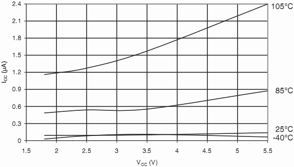
Bild 31-248: ATmega168PA: Stromaufnahme bei Leistung-weg vs. UCC (Watchdog aktiviert)

31.6.5 Stromaufnahme beim Leistung sparen
Bild 31-249: ATmega168PA: Stromaufnahme beim Leistung sparen vs. UCC (Watchdog deaktiviert und 32kHz Crystal Oscillator Running)

31.6.6 Stromaufnahme in Bereitschaft
Bild 31-250: ATmega168PA: Stromaufnahme in Bereitschaft vs. UCC (Watchdog deaktiviert)

31.6.7 Pin-Pullups
Bild 31-251: ATmega168PA: Strom durch Pullup-Widerstand vs. Eingangsspannung (UCC = 1,8 V)

Bild 31-252: ATmega168PA: Strom durch Pullup-Widerstand vs. Eingangsspannung (UCC = 2,7 V)

Bild 31-253: ATmega168PA: Strom durch Pullup-Widerstand vs. Eingangsspannung (UCC = 5 V)

Bild 31-254: ATmega168PA: Strom durch Pullup-Widerstand vs. Spannung am RESET-Pin (UCC = 1,8 V)

Bild 31-255: ATmega168PA: Strom durch Pullup-Widerstand vs. Spannung am RESET-Pin (UCC = 2,7 V)

Bild 31-256: ATmega168PA: Strom durch Pullup-Widerstand vs. Spannung am RESET-Pin (UCC = 5 V)

31.6.8 Treiberstärke der Pins
Bild 31-257: ATmega168PA: Ausgangsspannung vs. Strom nach Masse am I/O-Pin (UCC = 3 V)

Bild 31-258: ATmega168PA: Ausgangsspannung vs. Strom nach Masse am I/O-Pin (UCC = 5 V)

Bild 31-259: ATmega168PA: Ausgangsspannung vs. Strom von UCC am I/O-Pin (UCC = 3 V)

Bild 31-260: ATmega168PA Ausgangsspannung vs. Strom von UCC am I/O-Pin (UCC = 5 V)

31.6.9 Schaltschwelle und Hysterese der Pins
Bild 31-261: ATmega168PA Schaltschwelle vs. UCC (UIH, Pin liest „1“)

Bild 31-262: ATmega168PA Schaltschwelle vs. UCC (UIL, Pin liest „0“)

Bild 31-263: ATmega168PA Hysterese vs. UCC

Bild 31-264: ATmega168PA: Schaltschwelle vs. UCC am RESET-Pin (UIH, Pin liest „1“)

Bild 31-265: ATmega168PA: Schaltschwelle vs. UCC am RESET-Pin (UIL, Pin liest „0“)

Bild 31-266: ATmega168PA: Hysterese vs. UCC am RESET-Pin

31.6.10 Unterspannungsdetektor-Schwelle
Bild 31-267: ATmega168PA: Schaltschwellen des Unterspannungsdetektors vs. Temperatur (BODLEVEL = 1,8 V)

Bild 31-268: ATmega168PA: Schaltschwellen des Unterspannungsdetektors vs. Temperatur (BODLEVEL = 2,7 V)

Bild 31-269: ATmega168PA: Schaltschwellen des Unterspannungsdetektors vs. Temperatur (BODLEVEL = 4,3 V)

Bild 31-270: ATmega168PA: Kalibrierte Referenzspannung vs. Temperatur

Bild 31-271: ATmega168PA: Kalibrierte Referenzspannung vs. UCC

31.6.11 Interner Oszillator
Bild 31-272: ATmega168PA: Watchdog-Oszillatorfrequenz vs. Temperatur
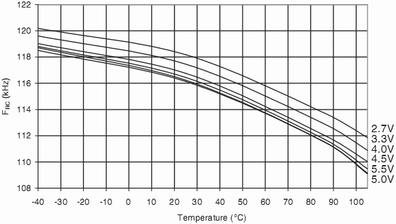
Bild 31-273: ATmega168PA: Watchdog-Oszillatorfrequenz vs. UCC

Bild 31-274: ATmega168PA: Kalibrierte 8-MHz-RC-Oszillatorfrequenz vs. UCC

Bild 31-275: ATmega168PA: Kalibrierte 8-MHz-RC-Oszillatorfrequenz vs. Temperatur

Bild 31-276: ATmega168PA: Kalibrierte 8-MHz-RC-Oszillatorfrequenz vs. OSCCAL-Wert

31.6.12 Verbrauch der I/O-Module
Bild 31-277: ATmega168PA: Stromaufnahme des A/D-Wandlers vs. UCC (AREF = AUCC)

Bild 31-278: ATmega168PA: Stromaufnahme des Analogvergleichers vs. UCC

Bild 31-279: ATmega168PA: Strom der externen Spannungsreferenz AREF vs. UCC

Bild 31-280: ATmega168PA: Stromaufnahme des Unterspannungsdetektor vs. UCC

Bild 31-281: ATmega168PA: Programmierstrom vs. UCC

31.6.13 Reset-Verbrauch und -Pulsbreite
Bild 31-282: ATmega168PA: Stromaufnahme während Reset vs. Frequenz (0,1 – 1,0 MHz)

Bild 31-283: ATmega168PA: Stromaufnahme während Reset vs. Frequenz (1 - 20 MHz)

Bild 31-284: ATmega168PA: Minimum Reset Pulse Width vs. UCC

31.7 Diagramme ATmega328
31.7.1 Strom unter Last
Bild 31-285: ATmega328: Strom unter Last vs. Frequenz (0,1 – 1,0 MHz)

Bild 31-286: ATmega328: Strom unter Last vs. Frequenz (1 – 20 MHz)
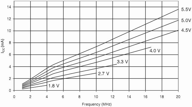
Bild 31-287: ATmega328: Strom unter Last vs. UCC (Interner RC-Oszillator, 128kHz)
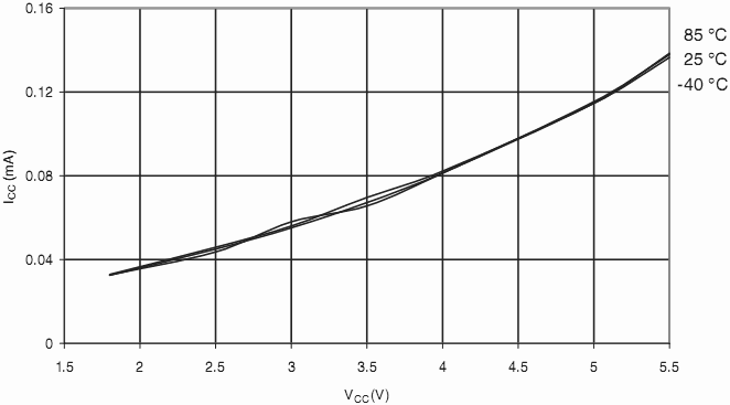
Bild 31-288: ATmega328: Strom unter Last vs. UCC (Interner RC-Oszillator, 1 MHz)

Bild 31-289: ATmega328: Strom unter Last vs. UCC (Interner RC-Oszillator, 8 MHz)

31.7.2 Stromaufnahme im Leerlauf
Bild 31-290: ATmega328: Stromaufnahme im Leerlauf vs. Frequenz (0,1 – 1,0 MHz)

Bild 31-291: ATmega328: Stromaufnahme im Leerlauf vs. Frequenz (1 – 20 MHz)

Bild 31-292: ATmega328: Stromaufnahme im Leerlauf vs. UCC (Interner RC-Oszillator, 128kHz)

Bild 31-293: ATmega328: Stromaufnahme im Leerlauf vs. UCC (Interner RC-Oszillator, 1 MHz)

Bild 31-294: ATmega328: Stromaufnahme im Leerlauf vs. UCC (Interner RC-Oszillator, 8 MHz)

31.7.3 ATmega328: Stromaufnahme der I/O-Module
Die folgenden Tabellen und Formeln können zur Berechnung der zusätzlichen Stromaufnahme der verschiedenen I/O-Module unter Last und im Leerlauf herangezogen werden.
Das Freigeben und Sperren der I/O-Module wird über das Leistungs-Reduktions-Register gesteuert.
Tabelle 31-13: ATmega328: Zusätzlicher Stromverbrauch der verschiedenen I/O-Module, in µA
| PRR-Bit | Typische Werte
|
|---|
| UCC = 2 V, F = 1 MHz | UCC = 3 V, F = 4 MHz | UCC = 5 V, F = 8 MHz
|
|---|
| PRUSART0 | 3,20 µA | 22,17 µA | 100,25 µA
|
| PRTWI | 7,34 µA | 46,55 µA | 199,25 µA
|
| PRTIM2 | 7,34 µA | 50,79 µA | 224,25 µA
|
| PRTIM1 | 6,19 µA | 41,25 µA | 176,25 µA
|
| PRTIM0 | 1,89 µA | 14,28 µA | 61,13 µA
|
| PRSPI | 6,94 µA | 43,84 µA | 186,50 µA
|
| PRADC | 8,66 µA | 61,80 µA | 295,38 µA
|
Tabelle 31-14: ATmega328: Zusätzlicher Stromverbrauch (in Prozent) unter Last und im Leerlauf
| PRR-Bit
| Zusätzlicher Stromverbrauch verglichen mit CPU-Last und externem Takt (siehe Bild 31-332 und Bild 31-333)
| Zusätzlicher Stromverbrauch verglichen mit Leerlauf und externem Takt (siehe Bild 31-337 und Bild 31-338)
|
|---|
| PRUSART0 | 1,4 % | 7,8 %
|
| PRTWI | 3,0 % | 16,6 %
|
| PRTIM2 | 3,3 % | 17,8 %
|
| PRTIM1 | 2,7 % | 14,5 %
|
| PRTIM0 | 0,9 % | 4,8 %
|
| PRSPI | 2,9 % | 15,7 %
|
| PRADC | 4,1 % | 22,1 %
|
It is possible to calculate the typical current consumption based on the numbers from Tabelle 31-13 for other UCC und frequency settings than listed in Tabelle 31-14.
31.7.3.1 Beispiel
Berechne die zu erwartende Stromaufnahme im Leerlauf mit TIMER1, ADU und SPI bei UCC = 2,0 V und F = 1 MHz:
Von Tabelle 31-14, dritte Spalte, we see that we need to add 14,5 % for the TIMER1, 22,1 % for
the ADU und 15,7 % for the SPI module. Reading from Bild 31-338, we find that the idle current
consumption is ≈0,055 mA at UCC = 2,0 V und F = 1 MHz. Die Gesamtstromaufnahme im Leerlauf mit
TIMER1, ADU und SPI enabled, gives:
ICCtotal ≈ 0,045 mA ∙(1 + 0,145 + 0,221 + 0.157) ≈ 0,069 mA
31.7.4 Stromaufnahme bei Leistung-weg
Bild 31-295: ATmega328: Stromaufnahme bei Leistung-weg vs. UCC (Watchdog deaktiviert)

Bild 31-296: ATmega328: Stromaufnahme bei Leistung-weg vs. UCC (Watchdog aktiviert)

31.7.5 Stromaufnahme beim Leistung sparen
Bild 31-297: ATmega328: Stromaufnahme beim Leistung sparen vs. UCC (Watchdog deaktiviert und 32kHz Crystal Oscillator Running)

31.7.6 Stromaufnahme in Bereitschaft
Bild 31-298: ATmega328: Stromaufnahme in Bereitschaft vs. UCC (Watchdog deaktiviert)
31.7.7 Pin-Pullups
Bild 31-299: ATmega328: Strom durch Pullup-Widerstand vs. Eingangsspannung (UCC = 1,8 V)

Bild 31-300: ATmega328: Strom durch Pullup-Widerstand vs. Eingangsspannung (UCC = 2,7 V)
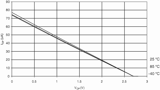
Bild 31-301: ATmega328: Strom durch Pullup-Widerstand vs. Eingangsspannung (UCC = 5 V)

Bild 31-302: ATmega328: Strom durch Pullup-Widerstand vs. Spannung am RESET-Pin (UCC =1.8 V)

Bild 31-303: ATmega328: Strom durch Pullup-Widerstand vs. Spannung am RESET-Pin (UCC =2.7 V)
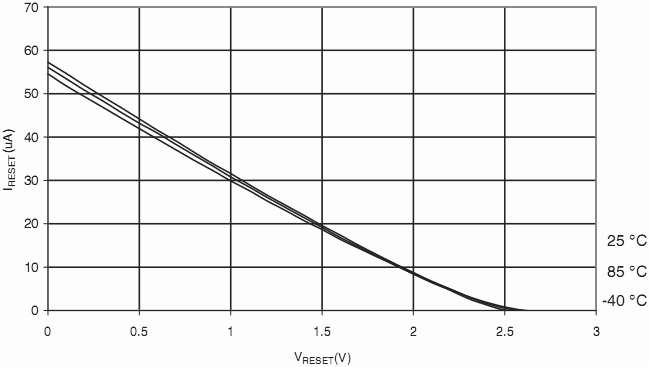
Bild 31-304: ATmega328: Strom durch Pullup-Widerstand vs. Spannung am RESET-Pin (UCC = 5 V)

31.7.8 Treiberstärke der Pins
Bild 31-305: ATmega328: Ausgangsspannung vs. Strom nach Masse am I/O-Pin (UCC = 3 V)

Bild 31-306: ATmega328: Ausgangsspannung vs. Strom nach Masse am I/O-Pin (UCC = 5 V)

Bild 31-307: ATmega328: Ausgangsspannung vs. Strom von UCC am I/O-Pin (UCC = 3 V)

Bild 31-308: ATmega328: Ausgangsspannung vs. Strom von UCC am I/O-Pin (UCC = 5 V)

31.7.9 Schaltschwelle und Hysterese der Pins
Bild 31-309: ATmega328: Schaltschwelle vs. UCC (UIH, Pin liest „1“)

Bild 31-310: ATmega328: Schaltschwelle vs. UCC (UIL, Pin liest „0“)

Bild 31-311: ATmega328: Hysterese vs. UCC

Bild 31-312: ATmega328: Schaltschwelle vs. UCC am RESET-Pin (UIH, Pin liest „1“)

Bild 31-313: ATmega328: Schaltschwelle vs. UCC am RESET-Pin (UIL, Pin liest „0“)

Bild 31-314: ATmega328: Hysterese vs. UCC am RESET-Pin

31.7.10 Unterspannungsdetektor-Schwelle
Bild 31-315: ATmega328: Schaltschwellen des Unterspannungsdetektors vs. Temperatur (BODLEVEL = 1,8 V)

Bild 31-316: ATmega328: Schaltschwellen des Unterspannungsdetektors vs. Temperatur (BODLEVEL = 2,7 V)
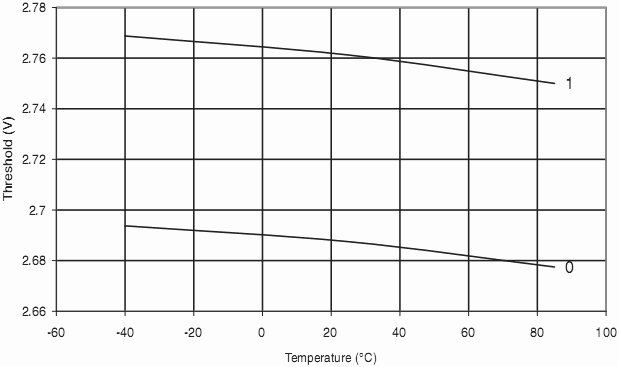
Bild 31-317: ATmega328: Schaltschwellen des Unterspannungsdetektors vs. Temperatur (BODLEVEL = 4,3 V)

Bild 31-318: ATmega328: Referenzspannung vs. UCC

31.7.11 Interner Oszillator
Bild 31-319: ATmega328: Watchdog-Oszillatorfrequenz vs. Temperatur

Bild 31-320: ATmega328: Watchdog-Oszillatorfrequenz vs. UCC

Bild 31-321: ATmega328: Kalibrierte 8-MHz-RC-Oszillatorfrequenz vs. UCC

Bild 31-322: ATmega328: Kalibrierte 8-MHz-RC-Oszillatorfrequenz vs. Temperatur

Bild 31-323: ATmega328: Kalibrierte 8-MHz-RC-Oszillatorfrequenz vs. OSCCAL-Wert

31.7.12 Verbrauch der I/O-Module
Bild 31-324: ATmega328: Stromaufnahme des A/D-Wandlers vs. UCC (AREF = AUCC)

Bild 31-325: ATmega328: Stromaufnahme des Analogvergleichers vs. UCC

Bild 31-326: ATmega328: Strom der externen Spannungsreferenz AREF vs. UCC

Bild 31-327: ATmega328: Stromaufnahme des Unterspannungsdetektor vs. UCC
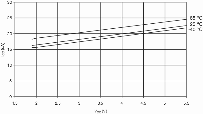
Bild 31-328: ATmega328: Programmierstrom vs. UCC

31.7.13 Reset-Verbrauch und -Pulsbreite
Bild 31-329: ATmega328: Stromaufnahme während Reset vs. Frequenz (0.1 - 1,0 MHz)

Bild 31-330: ATmega328: Stromaufnahme während Reset vs. Frequenz (1 - 20 MHz)

Bild 31-331: ATmega328: Minimale Resetpulsbreite vs. UCC
31.8 Diagramme ATmega328P
31.8.1 Strom unter Last
Bild 31-332: ATmega328P: Strom unter Last vs. Frequenz (0,1 – 1,0 MHz)

Bild 31-333: ATmega328P: Strom unter Last vs. Frequenz (1 – 20 MHz)

Bild 31-334: ATmega328P: Strom unter Last vs. UCC (Interner RC-Oszillator, 128kHz)

Bild 31-335: ATmega328P: Strom unter Last vs. UCC (Interner RC-Oszillator, 1 MHz)

Bild 31-336: ATmega328P: Strom unter Last vs. UCC (Interner RC-Oszillator, 8 MHz)

31.8.2 Stromaufnahme im Leerlauf
Bild 31-337: ATmega328P: Stromaufnahme im Leerlauf vs. Frequenz (0,1 – 1,0 MHz)

Bild 31-338: ATmega328P: Stromaufnahme im Leerlauf vs. Frequenz (1 – 20 MHz)

Bild 31-339: ATmega328P: Stromaufnahme im Leerlauf vs. UCC (Interner RC-Oszillator, 128kHz)

Bild 31-340: ATmega328P: Stromaufnahme im Leerlauf vs. UCC (Interner RC-Oszillator, 1 MHz)

Bild 31-341: ATmega328P Stromaufnahme im Leerlauf vs. UCC (Interner RC-Oszillator, 8 MHz)

31.8.3 ATmega328P Stromaufnahme der I/O-Module
Die folgenden Tabellen und Formeln können zur Berechnung der zusätzlichen Stromaufnahme der verschiedenen I/O-Module unter Last und im Leerlauf herangezogen werden.
Das Freigeben und Sperren der I/O-Module wird über das Leistungs-Reduktions-Register gesteuert.
Tabelle 31-15: ATmega328P: Zusätzlicher Stromverbrauch der verschiedenen I/O-Module, in µA
| PRR-Bit | Typische Werte
|
|---|
| UCC = 2 V, F = 1 MHz | UCC = 3 V, F = 4 MHz | UCC = 5 V, F = 8 MHz
|
|---|
| PRUSART0 | 3,20 µA | 22,17 µA | 100,25 µA
|
| PRTWI | 7,34 µA | 46,55 µA | 199,25 µA
|
| PRTIM2 | 7,34 µA | 50,79 µA | 224,25 µA
|
| PRTIM1 | 6,19 µA | 41,25 µA | 176,25 µA
|
| PRTIM0 | 1,89 µA | 14,28 µA | 61,13 µA
|
| PRSPI | 6,94 µA | 43,84 µA | 186,50 µA
|
| PRADC | 8,66 µA | 61,80 µA | 295,38 µA
|
Tabelle 31-16: ATmega328P: Zusätzlicher Stromverbrauch (in Prozent) unter Last und im Leerlauf
| PRR-Bit
| Zusätzlicher Stromverbrauch verglichen mit CPU-Last und externem Takt (siehe Bild 31-332 und Bild 31-333)
| Zusätzlicher Stromverbrauch verglichen mit Leerlauf und externem Takt (siehe Bild 31-337 und Bild 31-338)
|
|---|
| PRUSART0 | 1,4 % | 7,8 %
|
| PRTWI | 3,0 % | 16,6 %
|
| PRTIM2 | 3,3 % | 17,8 %
|
| PRTIM1 | 2,7 % | 14,5 %
|
| PRTIM0 | 0,9 % | 4,8 %
|
| PRSPI | 2,9 % | 15,7 %
|
| PRADC | 4,1 % | 22,1 %
|
It is possible to calculate the typical current consumption based on the numbers from Tabelle 31-15 for other UCC und frequency settings than listed in Tabelle 31-16.
31.8.3.1 Beispiel
Berechne die zu erwartende Stromaufnahme im Leerlauf mit TIMER1, ADU und SPI bei UCC = 2,0 V und F = 1 MHz:
Von Tabelle 31-16, dritte Spalte, we see that we need to add 14,5 % for the TIMER1, 22,1 % for
the ADU und 15,7 % for the SPI module. Reading from Bild 31-338, we find that the idle current
consumption is ≈0,055 mA at UCC = 2,0 V und F = 1 MHz. Die Gesamtstromaufnahme im Leerlauf mit
TIMER1, ADU und SPI enabled, gives:
ICCtotal ≈ 0,045 mA ∙(1 + 0,145 + 0,221 + 0.157) ≈ 0,069 mA
31.8.4 Stromaufnahme bei Leistung-weg
Bild 31-342: ATmega328P: Stromaufnahme bei Leistung-weg vs. UCC (Watchdog deaktiviert

Bild 31-343: ATmega328P: Stromaufnahme bei Leistung-weg vs. UCC (Watchdog aktiviert)

31.8.5 Stromaufnahme beim Leistung sparen
Bild 31-344: ATmega328P: Stromaufnahme beim Leistung sparen vs. UCC (Watchdog deaktiviert und 32kHz Crystal Oscillator Running)

31.8.6 Stromaufnahme in Bereitschaft
Bild 31-345: ATmega328P: Stromaufnahme in Bereitschaft vs. UCC (Watchdog deaktiviert)

31.8.7 Pin-Pullups
Bild 31-346: ATmega328P: Strom durch Pullup-Widerstand vs. Eingangsspannung (UCC = 1,8 V)

Bild 31-347: ATmega328P: Strom durch Pullup-Widerstand vs. Eingangsspannung (UCC = 2,7 V)
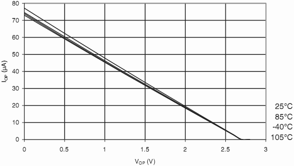
Bild 31-348: ATmega328P: Strom durch Pullup-Widerstand vs. Eingangsspannung (UCC = 5 V)

Bild 31-349: ATmega328P: Strom durch Pullup-Widerstand vs. Spannung am RESET-Pin (UCC = 1,8 V)

Bild 31-350: ATmega328P: Strom durch Pullup-Widerstand vs. Spannung am RESET-Pin (UCC = 2,7 V)

Bild 31-351: ATmega328P: Strom durch Pullup-Widerstand vs. Spannung am RESET-Pin (UCC = 5 V)

31.8.8 Treiberstärke der Pins
Bild 31-352: ATmega328P: Ausgangsspannung vs. Strom nach Masse am I/O-Pin (UCC = 3 V)

Bild 31-353: ATmega328P: Ausgangsspannung vs. Strom nach Masse am I/O-Pin (UCC = 5 V)

Bild 31-354: ATmega328P: Ausgangsspannung vs. Strom von UCC am I/O-Pin (UCC = 3 V)
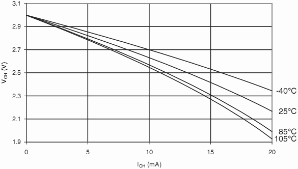
Bild 31-355: ATmega328P: Ausgangsspannung vs. Strom von UCC am I/O-Pin (UCC = 5 V)

31.8.9 Schaltschwelle und Hysterese der Pins
Bild 31-356: ATmega328P: Schaltschwelle vs. UCC (UIH, Pin liest „1“)

Bild 31-357: ATmega328P: Schaltschwelle vs. UCC (UIL, Pin liest „0“)

Bild 31-358: ATmega328P: Hysterese vs. UCC

Bild 31-359: ATmega328P: Schaltschwelle vs. UCC am RESET-Pin (UIH, Pin liest „1“)

Bild 31-360: ATmega328P: Schaltschwelle vs. UCC am RESET-Pin (UIL, Pin liest „0“)

Bild 31-361: ATmega328P: Hysterese vs. UCC am RESET-Pin

31.8.10 Unterspannungsdetektor-Schwelle
Bild 31-362: ATmega328P: Schaltschwellen des Unterspannungsdetektors vs. Temperatur (BODLEVEL = 1,8 V)

Bild 31-363: ATmega328P Schaltschwellen des Unterspannungsdetektors vs. Temperatur (BODLEVEL = 2,7 V)

Bild 31-364: ATmega328P Schaltschwellen des Unterspannungsdetektors vs. Temperatur (BODLEVEL = 4,3 V)

Bild 31-365: ATmega328P: Kalibrierte Referenzspannung vs. UCC

31.8.11 Interner Oszillator
Bild 31-366: ATmega328P: Watchdog-Oszillatorfrequenz vs. Temperatur

Bild 31-367: ATmega328PC Watchdog-Oszillatorfrequenz vs. UCC

Bild 31-368: ATmega328P: Kalibrierte 8-MHz-RC-Oszillatorfrequenz vs. UCC

Bild 31-369: ATmega328P: Kalibrierte 8-MHz-RC-Oszillatorfrequenz vs. Temperatur

Bild 31-370: ATmega328P Kalibrierte 8-MHz-RC-Oszillatorfrequenz vs. OSCCAL-Wert

31.8.12 Verbrauch der I/O-Module
Bild 31-371: ATmega328P: Stromaufnahme des A/D-Wandlers vs. UCC (AREF = AUCC)

Bild 31-372: ATmega328P: Stromaufnahme des Analogvergleichers vs. UCC

Bild 31-373: ATmega328P: Strom der externen Spannungsreferenz AREF vs. UCC

Bild 31-374: ATmega328P: Stromaufnahme des Unterspannungsdetektor vs. UCC

Bild 31-375: ATmega328P: Programmierstrom vs. UCC

31.8.13 Reset-Verbrauch und -Pulsbreite
Bild 31-376: ATmega328P: Stromaufnahme während Reset vs. Frequenz (0,1 – 1,0 MHz)

Bild 31-377: ATmega328P Stromaufnahme während Reset vs. Frequenz (1 - 20 MHz)

Bild 31-378: ATmega328P: Minimum Reset Pulse Width vs. UCC
